thin, white OLED in glass, (c) Fraunhofer FEP

WHAT IS ORGANIC ELECTRONICS?

Organic electronics facilitate the fabrication of novel, flexible, and large-area devices, which cannot be produced using conventional electronics. Transparent lighting elements, bendable displays, and lightweight photovoltaics are only a few examples for the versatility and immense potential this technology holds.

In this section, basic terms and the most important applications are explained comprehensively – an introduction to a new era of electronics and how we perceive them.

ORGANIC SEMICONDUCTORS

For the manufacturing of organic electronics, organic semiconductors are needed. The term organic is meant in a chemical way, distinguishing the used materials from inorganic ones used in conventional electronics. The most important building block for organic semiconducting small molecules, polymers, and thin-films is carbon, which present an ideal groundwork with the unique structures it forms.

Organic chemistry encompasses a multitude of material classes, many of which can be associated with living beings. Apart from a high water content we – humans, animals, plants, bacteria, etc. – are built almost exclusively from various hydrocarbons. Equally, lifeless materials like rubber, plastics, or gasoline count as organic. Considering how diverse the purposes and properties of these substances are, it does not surprise that the number of possibilities for electronic structures and attributes for organic semiconductors appears infinite as well.

ORGANIC SOLAR CELLS

Photovoltaic installations, turning sunlight into electrical energy, have become commonplace in our everyday life as well as the worldwide energy mix. However, with typical silicon solar cells we associate a certain color, high weight and troublesome mounts, accordingly. Organics shed new light on this concept outshine conventional solar panels: Lightweight, flexible, transparent, and in every imaginable color, organic solar cells fit everywhere – harvesting energy in completely new places.

Organic solar cells are deposited in extremely thin films using techniques which enable roll-to-roll production, the simplest example for which is a printing press. This way, a very high throughput is possible, reducing the cost of module production. Simple installation and light mounts further benefit the price. Lastly, these cells exhibit extremely short energy payback times from several weeks to few months, since there is no need for energy-intensive crystallization procedures as they occur in the production of conventional photovoltaics.

ORGANIC LIGHT EMITTING DIODES

The organic light emitting diode – OLED in short – is by far the most successful organic device, until now. Because of their low energy consumption and brilliant colors, active-matrix OLED (AMOLED) displays are being embedded in over 20% of all mobile phones worldwide, today. Increasing sales are also observed for OLED TVs, which are also ultra-thin and even curved due to the production process of organic devices in general. Furthermore, OLEDs also enable large-area lighting elements. The lightweight, flexible, and even semi-transparent modules are especially interesting for novel design concept, overcoming the limitations of conventional lighting elements. Beside fantasic light installations, rear signal lamps of car manufacturers Audi and BMW, have attracted a lot of attention.

OLEDs are not only a high-end product for TVs and car lighting. Printed on paper, they also refine products with rather short lifecycles such as packaging or business cards. This multiplies the usual product value by a strongly enhanced visibility. An OLED wallpaper could bathe living rooms in soothing full-area light. Unfortunately, this is not available – yet – but entirely possible in the near future.

ORGANIC SENSORS

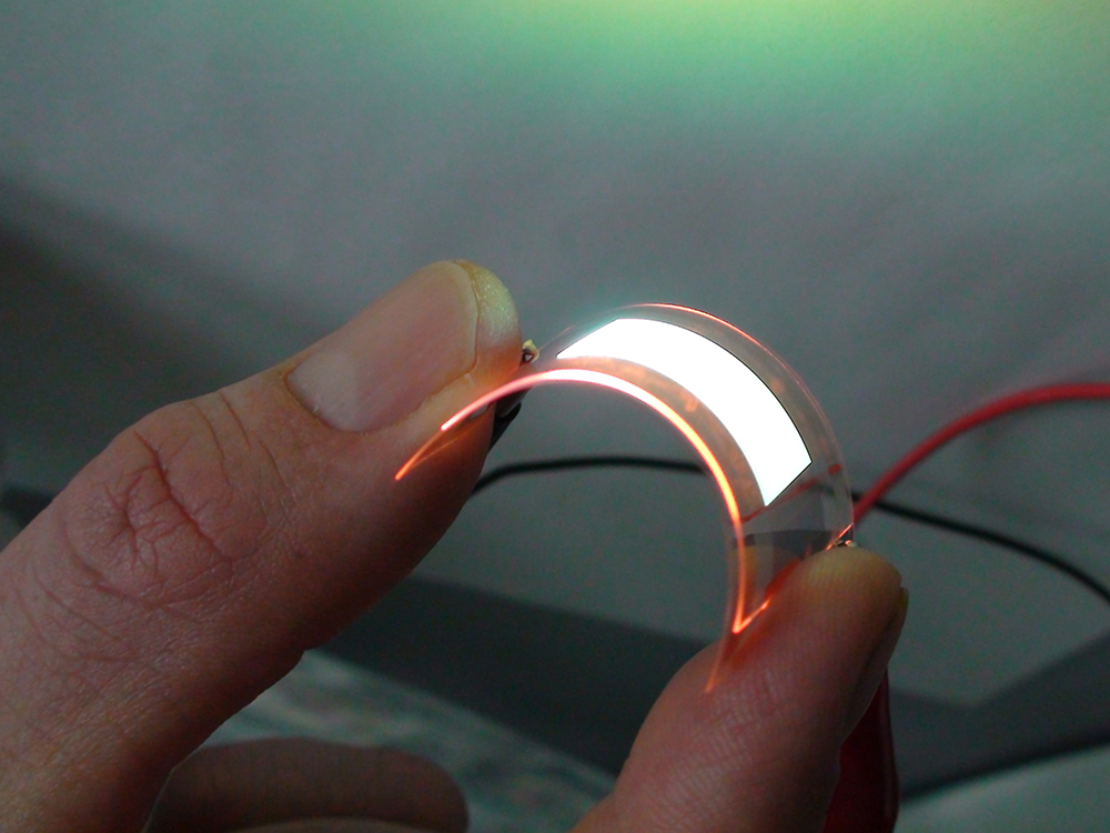
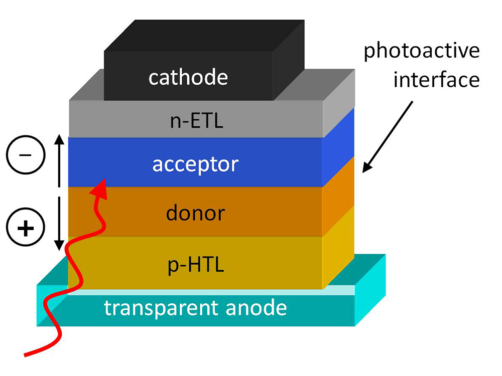
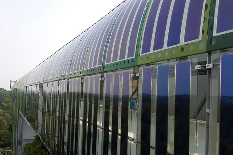
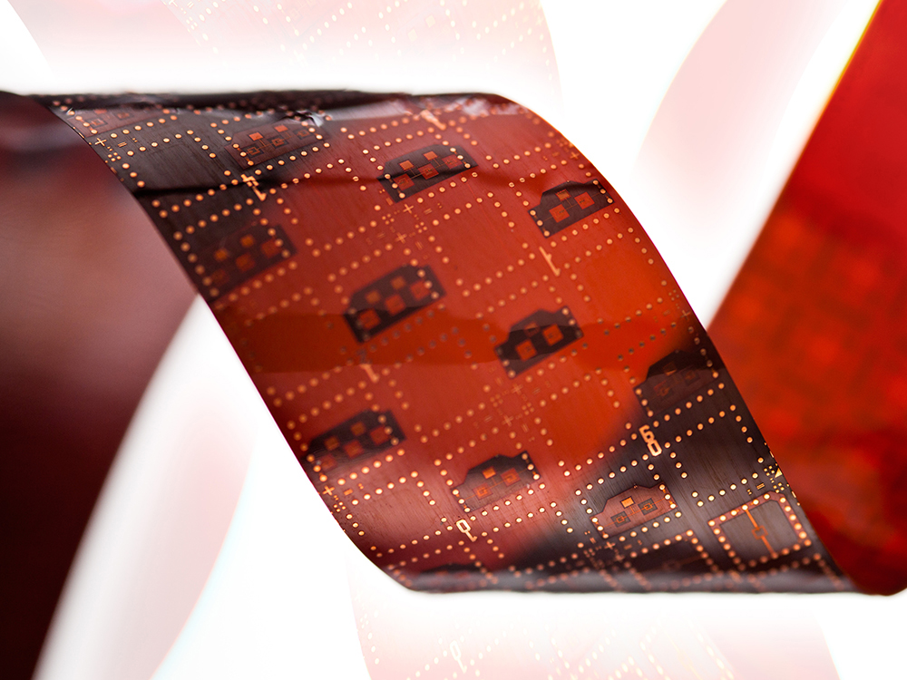
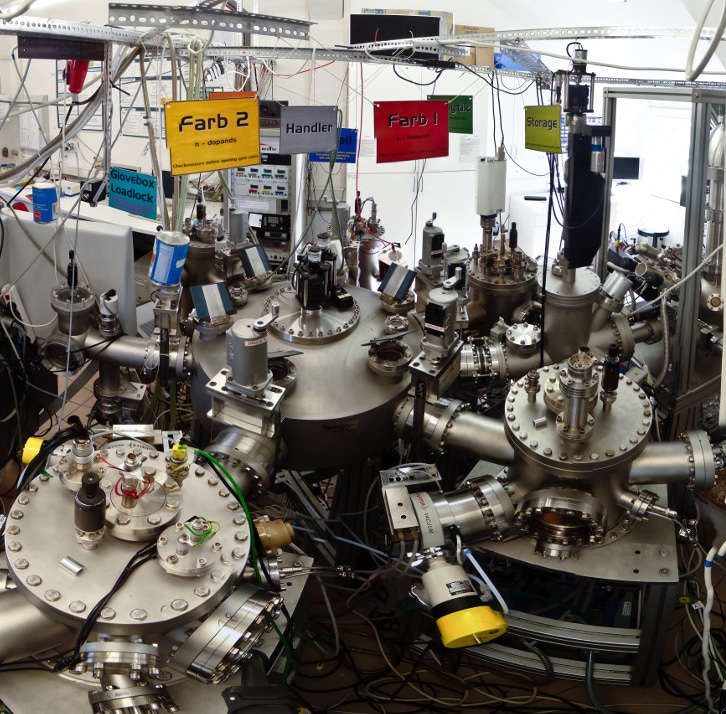
In the field of sensing, organic, flexible, large-area electronic solutions open up completely new possibilities. From photodetectors in the IR, visible, or X-ray spectrum to gas, pressure, or temperature sensors, they can convince with functionality and easy integration. Formerly packaged in rigid and bulky casings, they now fit seamlessly in textiles, paper, or plastic films. Heavy and expensive devices – such as NIR-detectors – become small, lightweight, and cost-effective, potentially revolutionizing health care and agricultural technology.

Solution-based processing

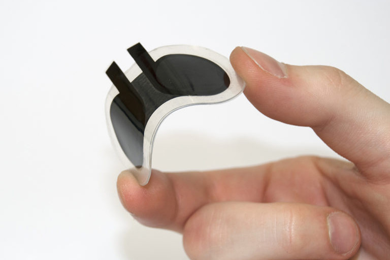
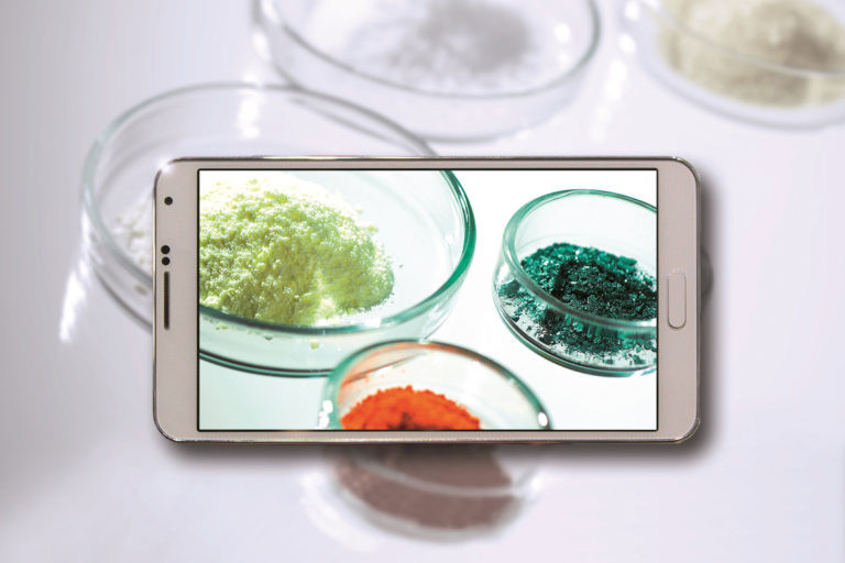
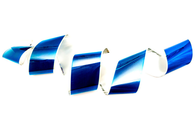
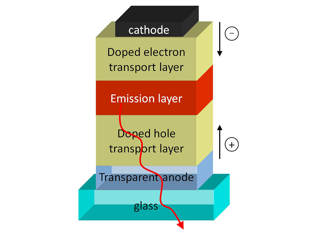
Solution-based processing is similar to printing with a conventional ink jet printer or a printing machine. The organic materials are dissolved in a liquid solvent, just like the color pigments in normal printer ink are dissolved in a liquid. Following this analogy, the solution is also referred to as ‘electronic ink’. This ink – carefully dosed – is applied to the substrate. The solvent is volatile, so once it has evaporated only the organic semiconductor remains on the substrate as a thin film.
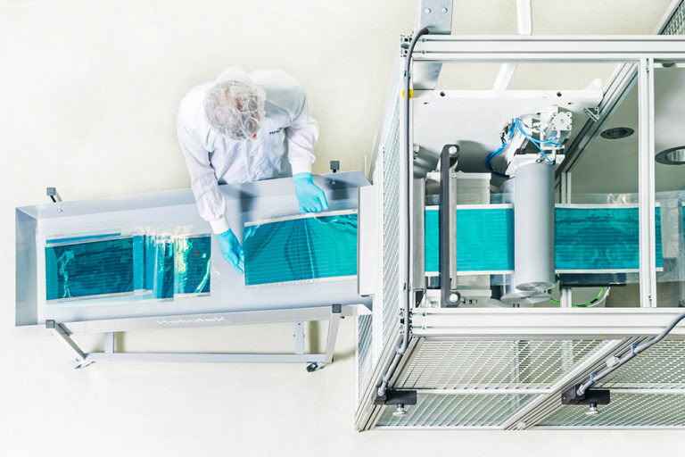
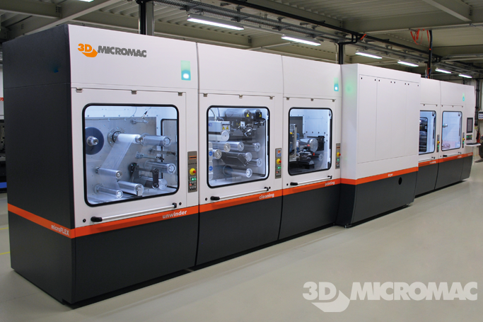
Solution-based processing is the simplest and technologically the most field-tested method for the fabrication of thin material films. It is suitable for processes in which films in the region of several micrometers or thicker are needed and where only one or very few layers of organic semiconductor are to be deposited. For components which comprise several clearly separated layers, specific combinations of organic semiconductors and solvents have to be used so that one film can be deposited onto an already existing one without etching this first film and thus causing an unwanted mixing of the two materials. Polymers (very large molecules) are often used here since they are less susceptible to solvents once they have been deposited. Processing on flexible substrates in a ‘roll to roll’ procedure is more easily possible, similar to newspaper printing machines.

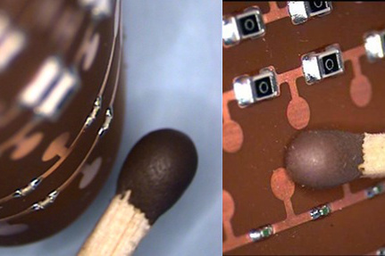
In times of digitalization and increasing connectivity, miniaturization and better integration of sensors become core aspects of their functionality. Pressure and temperature sensors on surgical gloves help during operations, NIR-detectors measure the ripeness of crops, and gas detectors in mobile phones or clothing assess air composition and issue warnings e. g. for dangerously high amounts of nitrogen oxides. Organic sensors enable the incorporation of invisible, unnoticeable functionality, anywhere.

ORGANIC TRANSISTORS

Transistors are everywhere and often times a lot more numerous than one might think. Reading these lines, chances are, billions of transistors currently surround you. Computer chips make up most of them, but every display, every sensor, every small logical circuit depends on transistors. One quickly realizes that the production of flexible displays or sensors cannot be done with conventional electronics. Organic electronics are able to address each pixel of a bendable display, amplify a sensor’s signal where it is generated, or perform simple logical operations – all using organic transistors.

Even though organic microchips could not compete with inorganic counterparts in terms of computing power, the roll-to-roll production of comparably simple logic circuits possesses remarkable advantages of its own. Not only transistors, but also organic diodes, resistors, capacitors, and inductors together enable the manufacturing of oscillators – the most basic elements of wireless communication. Low-cost mass production of logic and memory in combination with sensors integrated in packaging and tags generate an unprecedented benefit by individual tracking of single items and their environment.

FABRICATION OF ORGANIC DEVICES

Organic electronic devices mostly consist of organic semiconductors. These are powders or small cyrstals produced in chemical synthesis and deposited as extremely thin layers onto various  possible substrates. There is no need to produce big, perfect crystals or etch structures into rigid wafers. Such organic powders are either solved and applied in a wet process or evaporated in vacuum – both processes allow for roll-to-roll production. Necessery structures are either created with masks, laser cuts, or directly by selective deposition using certain printing techniques.

If a material can be deposited in a wet process, in vacuum, or both depends on ist chemical structure. The bigger and heavier the molecule, the lower the probability of successful vacuum evaporation. Therefore, substances for vacuum processing are often referred to as „small molecules“. Molecules of any size can be solved – but only if they possess the correct chemical side groups. Materials used for this purpose are mostly polymers.

Both vacuum and solution-based device fabrication have advatages and disadvantages for practical use. For vacuum processing, a deposition chamber needs to be evacuated, first. During solution processing, the deposition system needs to be vented carefully due to large amounts of solvent vapors. In vacuum deposition, a potentially infinite amount of single layers can be evaporated subsequently without the danger of once again solving previously deposited thin-films. However, they need structuring by shadowmasks or lasers while many printing tehniques allow for selective deposition, natively. While logic and sensors are currently deposited in wet processes for the most part, OLED displays are exclusively fabricated in vacuum. For organic solar cells, both methods are practiced.

HOW IT WORKS

Organic semiconducting molecules utilize the structure of their carbon backbone, which grants them unique electronic properties. In a honeycomb-like assembly, a so-called extended pi system forms, which gets its name from the chemical pi bond between atoms. Electrons are able to move quite freely in here, making the molecule semiconducting. In order to further increase conductivity, small molecules can be doped with other molecules. If their electronic properties are compatible, additional free charge carriers are generated in a mixed layer of both.

Organic devices like OLEDs or organic solar cells are called excitonic devices. When light is absorbed in a solar cell, an organic molecule changed into an excited state. Compared to inorganic electronics, this state is quite stable and diffuses through the layer stack by hopping from one molecule to another – this is the so-called exciton. Controlling these quasi particles is a core challenge in all organic devices: In organic solar cells, excitons have to be transformed to free charge carriers to make use of the light’s energy. In OLEDs on the other hand, excitons are created from free charge carriers. After some time, they become instable and emits its stored energy as light – the OLED lights up.